
Solderability Testing
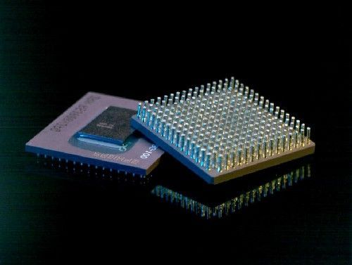
CGA Components
A solderability test determines whether component leads and device package terminations can be wetted by molten solder. Six Sigma Microelectronics performs solderability testing on electronic components to IPC J-STD-002 and MIL-STD-883 Method 2003, using the dip and look method for leaded and leadless parts and surface mount simulation for BGAs, CGAs and other surface mount devices where dip and look is not appropriate. Solderability testing is a destructive test — tested components are consumed and must not be installed in final assemblies. For forty years we have performed this work for defense and space programs where one unreliable solder joint is not an acceptable outcome.
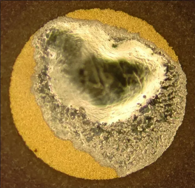
Good wetting, dewetting, and non-wetting on an LGA pad
What Is a Solderability Test?
A solderability test determines whether component leads and device package terminations can be wetted by molten solder. Solderability testing applies accelerated aging, immerses test samples in a solder bath, and inspects the resulting solder coating against defined acceptance criteria. Solderability testing is a destructive test — tested electronic components must not be installed in final assemblies.
During the 1980s and early 1990s, engineers at IBM and Raychem pioneered compliant solder column interconnect technology to address the limitations of conventional solder ball attachments. Traditional Ball Grid Array (BGA) solder spheres often experienced fatigue-related failures when subjected to repeated thermal cycling, particularly when large ceramic packages were mounted to organic printed circuit boards.
Solderability is the ability of a solderable surface to be wetted by molten solder. Wetting is the behavior that matters: molten solder must flow across the metal and form a continuous, adherent film rather than beading up and pulling away. Solder wettability describes how readily a given surface does this. When a termination has lost that ability — usually to oxidation or contamination — the solder will not bond properly, and no amount of process control on the assembly line will recover it.
The test does not evaluate the component's electrical function. It evaluates one property: whether the surface will accept solder. That is why the test is destructive, and why it is performed on test samples drawn from the lot rather than on the parts destined for the build.
Why Solderability Testing Matters
Poor solderability produces solder joint defects that are expensive to find late and expensive to fix. Non wetting and dewetting are the two most common — solder that never adheres, and solder that adheres and then withdraws. Both leave a mechanically weak joint that can pass a casual visual inspection and fail later under thermal cycling or vibration.
In electronics production the real cost sits in the sequence. Screening incoming parts is a controlled expense. Finding the same problem after the parts are populated means costly rework. Finding it after the module is built often means replacing complete electronic assemblies. Early identification of solderability failures saves significantly compared with replacing finished hardware.
Solderability testing functions as a quality control gate. It detects surface oxidation, contamination, plating defects and coating degradation before parts reach the final assembly line, and it identifies the specific conditions that lead to poor solder adhesion — while the only thing at risk is the sample.
For high reliability applications the calculation changes again. Reliable solder joints determine the long term performance of the assembly, and in space and defense hardware there is no service call after delivery. The risk being managed is not first-pass yield. It is the flight article.

Solderability screening for stored and legacy parts
Components pulled from long term storage, from bonded stock, or from the obsolete market arrive with an unknown surface condition. Solderability screening confirms those parts remain assembly-ready and will not fail at next level assembly because of an un-wettable oxide layer. This is the most common reason parts are sent to us for solderability testing.
What Causes Solderability to Degrade
A component leaves its manufacturer solderable. What happens between that moment and the assembly line is what a solderability test is designed to detect. Poor surface finishes, aggressive storage conditions and simple elapsed time are the three drivers.
Surface finish and shelf life
The surface finish applied to component terminations and to printed circuit board lands significantly affects both initial solderability and practical shelf life. HASL gives a robust, solder-compatible surface with a long shelf life but an uneven topography. ENIG gives a flat, planar surface well suited to fine pitch parts, at the cost of sensitivity to nickel corrosion. OSP — organic solderability preservative — is a thin organic coating that protects copper but degrades with handling and thermal exposure. Immersion Silver and Immersion Tin both perform well when fresh; Immersion Silver is prone to tarnish, and Immersion Tin to intermetallic growth that consumes the tin layer over time. Each finish carries distinct advantages and disadvantages, and each ages on its own schedule.
Storage conditions
Temperature, humidity and atmosphere drive the rate at which solderability degrades. Higher humidity and higher temperature accelerate oxidation and corrosion. Storage conditions adequate for six months are frequently not adequate for six years. Packaging materials matter as well — dry pack, desiccant and moisture barrier bags slow the process without stopping it, and a bag that has been opened once has a different history from one that never was.
Oxidation and intermetallic growth
Two distinct mechanisms are at work here, and they are often conflated.
Oxidation is a surface phenomenon. Exposed metal forms an oxide layer that inhibits wetting. Flux is designed to reduce that layer during soldering, but past a certain thickness the flux activity available in a normal assembly process is not enough, and the solder will not adhere.
Intermetallic growth is a bulk phenomenon. At the boundary between the solderable layer — usually tin — and the base metal beneath it, an intermetallic compound forms and grows. As it grows it consumes the solderable layer. When the intermetallic reaches the surface there is no solderable material left to wet, and any joint that does form is brittle. This is why a part can look perfectly acceptable and still be unsolderable.

Image Placeholder
Preconditioning: Steam Aging and Dry Bake
Steam aging is an accelerated aging step performed before a solderability test. Steam conditioning exposes test samples to saturated water vapor to simulate the surface oxidation that develops during long term storage and shipping. Dry bake serves as an alternative preconditioning method. Preconditioning is what makes a solderability test predictive of assembly performance after warehouse shelf life.
Without preconditioning, a solderability test answers only one question: was this part solderable on the day it was tested. That is rarely the question a program office is asking. The question is whether the part will still be solderable when it reaches the assembly floor, after however long it sits in storage first.
Accelerated aging answers that question. Steam conditioning compresses the natural degradation, shelf-life limitation and environmental exposure of warehouse storage and shipping into a controlled interval. The applicable standard specifies which preconditioning category applies to which component finish, and the category selected changes the severity of the test.
Each project is reviewed by experienced personnel to ensure compatibility with customer requirements, reliability objectives, and end-use environments.
Solderability Test Methods
Three methods are in general use. Which one applies is determined by the component package, not by preference.
Dip and look test
The dip and look test is a qualitative solderability test method. Test samples receive steam conditioning, then activated rosin flux, then a controlled immersion in a solder pot using a dipping mechanism. After dipping, a low power microscope inspects each termination for a smooth, adherent film of solder and for base metal exposed by non wetting or dewetting.
Every variable in that procedure is controlled: flux activity, solder bath temperature and composition, the immersion and withdrawal rate of the dipping mechanism, and dwell time in the dip. A solder pot running off temperature, or a flux more aggressive than the standard specifies, will pass parts that should have failed. The discipline is in the setup, not the dip.
Inspection is where the judgment sits. The inspector looks for continuous coverage of the solderable surface. Pinholes, voids, non wetting, dewetting and base metal exposed through the coating all count against the minimum acceptance criteria in the applicable standard.
The method's value is its simplicity, low cost and speed. Its limitation is that it produces no numerical output. A part passes or it does not.
Image Placeholder
Surface mount simulation test
The surface mount simulation test evaluates surface mount components that the dip and look method cannot assess, including BGAs and CGAs. Solder paste is screen printed onto a ceramic plate or FR-4 substrate, the component is placed onto the paste, and a specified convection reflow profile is run. Inspection then follows the specified acceptance criteria.
The reason the method exists is straightforward. A BGA or CGA has no lead to dip. Its terminations are solder balls or columns on the underside of the package, and immersing that package in a solder pot says nothing useful about how it will behave in a reflow oven. Surface mount simulation reproduces the process the part will actually see — paste, placement, thermal profile — and evaluates the result against that process.
This is adjacent to work we perform every day. Six Sigma attaches columns and balls to these packages. Testing their solderability under a real reflow profile is the same discipline turned toward inspection.
Wetting balance analysis
Wetting balance analysis is a quantitative solderability test method. A test specimen is immersed in a molten solder bath while the instrument records the vertical wetting force acting on the specimen over time. The resulting wetting curve gives numerical time-to-wet and maximum wetting force values, where the dip and look method returns only a visual pass or fail.
The wetting balance test is governed by standards including IEC 60068-2-69 and J-STD-002. Because the output is measured rather than observed, wetting balance analysis is the right tool when the objective is comparison — one surface finish against another, one supplier against another, one date code against another — rather than a straightforward accept or reject decision.
Placeholder image
Image Placeholder
Choosing a method
| Method | Output | What it evaluates | Best suited to | Destructive |
|---|---|---|---|---|
| Dip and look | Qualitative — visual pass or fail | Solder coverage and adherence after controlled immersio | Leaded and leadless components; fast screening of incoming lots | Yes |
| Surface mount simulation | Qualitative — visual pass or fail after reflow | Wetting behavior under an actual reflow profile | All surface mount components, including BGAs and CGAs | Yes |
| Wetting balance analysis | Quantitative — wetting curve, time-to-wet, wetting force | Vertical wetting force over time during immersion | Comparing finishes, suppliers or date codes | Yes |
Standards We Test To
Component solderability is governed by a small set of industry standards. The controlling document is whichever one your drawing or purchase order calls out.
IPC J-STD-002
IPC J-STD-002 is the primary industry standard for testing the solderability of component leads, terminations, lugs, terminals and wires. The standard prescribes the test methods, defines the defects, and sets the acceptance criteria used to verify solderability. Its test designations cover leaded parts, leadless parts, wire, wetting balance methods and surface mount process simulation, so a single standard governs nearly every package type we handle.
MIL-STD-883 Method 2003
MIL-STD-883 Method 2003 evaluates the solderability of microcircuit device package terminations intended to be joined to another surface by SnPb eutectic solder at next level assembly. The method specifies steam aging and flux application, and references J-STD-002 for detailed procedure. Method 2003 defines preconditioning by category: Category 2 covers non-tin component finishes excluding gold; Category 3 covers all other finishes, including gold, and requires the longer steam preconditioning. Method 2003 is the method most often cited on our defense and space customers' drawings.
MIL-STD-202 Method 208
MIL-STD-202 Method 208 is the solderability test method applied to electronic component parts under MIL-STD-202.
A note on lead free assembly
SnPb and lead free solder processes are not interchangeable for test purposes. MIL-STD-883 Method 2003 is written for SnPb eutectic assembly. Where parts are intended for a Pb free solder process, the test conditions and the preconditioning category must reflect that. Confirm the intended assembly alloy when you submit parts, and we will test to it.
What J-STD-003 covers, and what it does not
IPC J-STD-003 covers the solderability of printed board surface conductors and attachment lands, providing methods and criteria to confirm that fabrication and storage have not adversely affected solderability. J-STD-003 is a printed circuit board standard. Six Sigma tests components and device package terminations under J-STD-002 and MIL-STD-883 — PCB solderability under J-STD-003 is a separate scope, noted here only so there is no confusion about what we test.
Image Placeholder
Solderability Testing at Six Sigma Microelectronics
Six Sigma Microelectronics has performed microelectronics soldering work for forty years, for defense and space programs where reliability and precision are not negotiable, and that work carries a substantial flight heritage. Solderability testing sits alongside the services it most often supports — Column Attach, Ball Attach and Hot Solder Dip — and alongside the analytical capabilities we use when a result needs to be understood rather than simply recorded: 3D X-ray, acoustic microscopy, scanning electron microscopy and metallographic cross-sectioning.
That combination matters when a lot fails. A solderability test tells you a part did not wet. Cross-sectioning and SEM tell you why it did not, which is the difference between rejecting a lot and fixing a supply problem.
Send us the part number, the lot size and the controlling standard, and we will tell you which method applies and what it will take.
Frequently Asked Questions
What is solderability?
Solderability is the ability of a metal surface to be wetted by molten solder. A solderable surface allows molten solder to flow across it and form a continuous, adherent film. Surface oxidation, contamination and plating defects all reduce solderability, and a termination that has lost solderability will not form a reliable solder joint.
Is solderability testing destructive?
Yes. Solderability testing is a destructive test. Test samples are immersed in molten solder or run through a full reflow profile, and the parts are consumed in the process. Tested electronic components must not be installed in final products. Sample quantity is drawn from the lot according to the applicable standard.
What is the difference between the dip and look test and wetting balance analysis?
The dip and look test is qualitative: a termination is dipped in a solder pot and inspected under a low power microscope for a smooth, adherent film of solder. Wetting balance analysis is quantitative: the wetting force acting on a test specimen is measured over time and plotted as a wetting curve, producing numerical time-to-wet and maximum force values.
Which standard applies to my parts — J-STD-002 or MIL-STD-883 Method 2003?
The controlling document is your drawing or purchase order. IPC J-STD-002 is the general industry standard for component lead and termination solderability. MIL-STD-883 Method 2003 applies to microcircuit device package terminations for SnPb eutectic solder assembly and is common on defense and space programs. Method 2003 references J-STD-002 for detailed procedure.
How many samples are required for a solderability test?
Sample size is specified by the applicable standard and by the size of the lot being screened. Because solderability testing is a destructive test, sample quantity should be agreed before parts are shipped. Send the part number, the lot size and the controlling standard and we will confirm the requirement.